
Latest Search

Quote
| Back Zoom + Zoom - | ||||
|
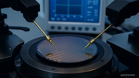
Mainland CN's First 12-Inch Silicon Photonics Chip Platform Officially Launched
Recommend 17 Positive 34 Negative 10 |
||||
|
||||
|
China's first domestically produced silicon photonics PDK (Process Design Kit), TDK (Test Design Kit), and ADK (Assembly Design Kit) based on a 12-inch 40nm CMOS process line has officially been launched in Wuhan Donghu New Technology Development Zone (China's Optics Valley), according to the WeChat public account of "China Optics Valley". This platform provides full-process support from chip integration design to packaging verification, meeting the rapid iteration needs in the transformation of scientific research achievements and product development. The platform is constructed and operated by the National Optoelectronics Innovation Center (NOEIC). It innovatively establishes a silicon photonics MPW (Multi-Project Wafer) service model, integrating multiple chip designs on the same wafer to achieve cost-sharing and sharply lower R&D barriers. AASTOCKS Financial News Website: www.aastocks.com |
||||
|
Copied to Clipboard
 |
||||